Arduino-YourDuino-MEGA2560-1280
Arduino / YourDuino MEGA 1280 and 2560 Overview:
Based on material from HiTechHiTouch.


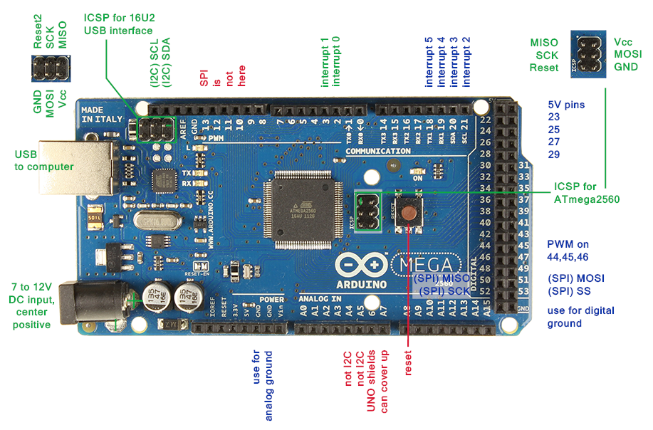
  Arduino Mega2560 Revision 3 board picture (Above)
Board Revisions:
Revision 2 of the Mega ADK board has a resistor pulling the 8U2 HWB line to ground, making it easier to put into DFU mode. This is for upgrading the USB support chip, a most infrequent event.
  Revision 3 of the board has the following new features:
- Two SCL and SDA pins to the left of the AREF pin for easy I2C access.
- Two new pins at the left of the RESET pin. The left most is reserved for future use. IOREF, next to RESET, allows shields to see if the attached board is an Arduino running a 5V, or a newer 3.3V board such as an Arduino Due.
- Stronger RESET circuit. This allows a reset to be done by temporarily shorting the power pins.
Voltage and Speed
The board runs at 16 MHz and 5 volts. (Older MEGAs ran at 8 MHz for Arduino compatibility.) Operating at 3.3 V is not possible (even if you supply 3.3V to Vin) because the MEGA 256 requires the higher 5V to run faster than 8 MHz, and the oscillator is fixed at 16 MHz.
CONNECTING POWER:
The board can be powered three ways:
- The USB connector (5V), which will also power several electronic bricks or homebrew devices. A self-resetting fuse limits current drawn through the USB connector to 500 mA, the USB1 standard. USB power (but not the USB signal) is electronically disconnected when power is supplied using the DC power jack or VIN pin. USB supplied 5V is used directly without conditioning.
- The DC power jack (7 - 12V), which takes a DC coaxial power plug 6.0 mm OD by 2.1mm ID, positive voltage center pin. A diode protects the board if you accidentally use a negative center pin.
- The VIN pin of the board (7-12V). Power from the DC power jack is sent to the VIN pin, so don't use the DC power jack if you supply power to VIN. Also, there is no diode to protect against reverse polarity. If you don't use a wall-wart with a coaxial plug, we recommend wiring the external supply leads into a plug so you can use the DC power jack and never using VIN.
The DC power jack / VIN pin feeds a regulator that generates 5V for the board, thus allowing the extended input voltage range. The regulator has over-current protection, and will shut down at 1A or if it gets too hot. The voltage cost of regulation is why the 7 volts minimum input is required.
A separate regulator provides 3.3 volts, limited to a maximum current draw of 50 mA.
The 5V and 3.3V pins are meant to deliver power out to circuits and devices you connect to the Mega. Using them to supply voltage into the board bypasses the regulators, and can damage your board. We don't advise it.
Using Batteries
The basic board will probably draw around 350mA. This can be quite a load for AA alkaline batteries, so consider larger size "C" or "D" cells, or specialized Li-Ion cells. Here are some good discussions about batteries, and here are some battery holders.

  Connecting batteries using the VIN pin to bypass the regulator has two advantages and two dangers. The regulator adds a significant voltage drop, which is why the DC power jack is specified as 7V minimum when the board only needs 5V. It also demands more total power from the batteries, so bypassing it can lower the drain on the batteries. The disadvantages are that there is no protection for battery combinations that deliver more than 5 volts, and there is no protection if you accidentally hook batteries up backwards to VIN and ground.

  Battery power is clean and stable, so the regulator is not useful when you supply 5V from batteries. Four Ni-Cad cells at 1.2V each totals 4.8 volts which will work well, as will lithium cells at or just below 5V.
  4.5V (e.g. three alkaline 1.5V cells in series) will run the board for a while, but things will flake out well before the end of the battery's life. Avoid this and the intermittent low voltage failure headaches.

 Warning: 6 volts, (e.g. four alkaline 1.5V cells in series) is too much for direct connection to "5V", and without the regulator there is no protection against cooking your board. Hooking 6 volts up using the regulator (DC Power jack) won't leave the voltage high enough for reliable operation after the regulator extracts its voltage drop. You will need five, not four, cells in series delivering 7.5 volts to use the DC Power jack.
INPUT AND OUTPUT:
Each of the 54 digital pins on the Mega can be used as an input or output, using pinMode(), digitalWrite(), and digitalRead() functions. They operate at 5 volts. Each pin can provide or receive an absolute maximum of 40 mA (20 mA recommended) and has an internal pull-up resistor (disconnected by default) of 20-50 K ohms. (The manufacturing process doesn't allow ATMEL to give precise pull-up values.)

  For Details see THIS page.
Absolute Maximum ratings:
DC Current per I/O Pin ............................................... 40.0 mA
  DC Current VCC and GND Pins................................ 200.0 mA

  The good news is that you get 800mA to play with, as there are 4 Vcc and 4 Gnd pins. The bad news is that there are multiple Vcc and Gnd pins on the chip, and one can't push all 800 mA through just one of them. As long as you respect the source/sink group limitations, there will be no problems. If you truly want to push a lot of current, spread it evenly around and expect the chip to run hot!

  The rating/test condition [(20mA at Vcc = 5V) under steady state conditions (non-transient)] uses just a single pin. In other words, you aren't guaranteed to get the full power limit across all pins if any pin is drawing more than 20 mA at 5V. Pushing past this limit to consistently get the maximum 40mA on a pin can severely shorten the life of the chip.

  Power draw is further limited by groups of pins for sink (IOL) and source (IOH) current. The total current from all pins in each group must stay under the maximum for the group.
Pin SOURCE and SINK Current Limitations (IOH/IOL):
| Group |
ARM Mega port labels |
Max Current |
Arduino Pin Labels |
| 1 |
J0-J7, A0-A7, G2 |
<= 200 mA |
Digital 14-15, 22-29, 39. |
| 2 |
C0-C7, G0-G1, D0-D7, L0-L7 |
<= 200 mA |
Digital 30-37, 40-41, 18-21, 38, 42-49. |
| 3 |
G3-G4, B0-B7, H0-H7 |
<= 200 mA |
Digital u-u, 50-53, 10-13, 16-17. |
| 4 |
E0-E7, G5 |
<= 100 mA |
Digital 0-3, 5, 4. |
| 5 |
F0-F7, K0-K7 |
<= 100 mA |
Analog A1-8, A9-15. |
Interestingly enough, the Arduino design team selected a voltage regulator that limits the current draw through the DC power jack to 1A (1000mA). Figure 800mA for the chip, and 200mA for the support circuitry and connected devices... Do try to live within their power budget!
Logic Level Details
Low level (logical zero) is under 0.3V, down to -0.5V. (Watch when connecting CMOS devices, especially devices running less than 4.5 Vdd.)

  High level (logical one) is from .6V, up to 5.5V. (Stay under 5 V!). CMOS devices generally need a slightly higher voltage to count as "high". Connect 74HCT family devices (instead of 74HC) as they are designed to solve this problem. Here is more information on level matching.

  The I/O pins on the mega start in "input" mode at reset/power up and then can have their function changed in the sketch with the pinmode() function. Input is a high impedance setting, which will be observed as a high level by a device expecting to receive input from the pin.

  Digital pin 13 is an exception as the boot-loader temporarily uses it as output to flash the LED. If you need Pin 13 connected to Power or Ground, you should go through a 1k current limiting resistor to protect the LED.
  Pin 13 is also harder to use as a digital input than the other digital pins because it has an LED and attached resistor are soldered to the board. If you enable its internal pull-up resistor, it will hang at around 1.7V instead of the expected 5V because the onboard LED and series resistor pull the voltage level down, meaning it always returns LOW. If you must use pin 13 as a digital input, set its pinMode() to INPUT, disable the internal pull-up, and use an external pull down resistor over 1.2K ohms.

  The I/O Pin internal pull-up resistor is 20K - 50K, ohm; (ATMEL gives only a range). The calculated minimum value for an external is 1.5K. Go high to conserve power; go low when transition speed and noise immunity is paramount. Without a pull up resistor, unconnected input pins will spontaneously change values. You must explicitly enable the internal pull-up using pinmode(n,INPUT_PULLUP).

  CMOS and TTL connections are push-pull (source and sink current), which always require pull-ups (exceptions apply when directly connecting CMOS) unless they are used as "tri-state" or "open collectors". The pinmode(n,INPUT) function puts a pin into open collector mode.

  Open collector is used to connect to a shared data bus with multiple devices or two-way conversations, similar to a telephone party line. When it is your turn use the bus, you expect the other devices to set their connection to open collector so they don't interfere. Then you set your pin(s) INPUT_PULLUP or OUTPUT, and the device you're talking to sets their pin(s) to output or input. Reverse the settings to talk the other way. Controlling who does what when on the bus is a (project) design matter, and often uses additional bus control lines.
Analog Output
There is no Digital to Analog converter on the chip. You cannot set and hold a specific output voltage. The (misnomered) AnalogWrite() function actually writes a burst of pulses at 490 hertz with a duty cycle specified by the AnalogWrite() parameter. This is known as Pulse Width Modulation.

  Creating a true analog output signal (e.g. audio) requires external circuitry to shape the pulse train. Consult Analog-Output for more information.
SPECIALIZED FUNCTIONS:
RESET: Bring this line LOW to reset the microcontroller. Typically used to add a reset button to shields which cover the reset button on the mega-board, or by a "watch dog" circuit to restart things after an assumed fault.
Serial 0: 0 (RX) and 1 (TX); Serial 1: 19 (RX) and 18 (TX); Serial 2: 17 (RX) and 16 (TX); Serial 3: 15 (RX) and 14 (TX). Used to receive (RX) and transmit (TX) TTL serial data. Pins 0 and 1 are also connected to the USB-to-TTL Serial chip, so the USB connected device (e.g. a PC) appears at Serial 0.
External Interrupts: pins 2 (interrupt 0), 3 (interrupt 1), 18 (interrupt 5), 19 (interrupt 4), 20 (interrupt 3), and 21 (interrupt 2). These pins can be configured to trigger an interrupt on a low value, a rising or falling edge, or a change in value. See the attachInterrupt() function for details.
PWM: pins 2 to 13 and 44 to 46. Provide 8-bit PWM output with the analogWrite() function. Pulse Width Modulation is a variable duty cycle square wave that provides power proportional to the percentage of time the wave is at its high value. The Mega square wave frequency is 490 Hz; other Arduino family members have a different frequency.
SPI: pins 50 (MISO), 51 (MOSI), 52 (SCK), 53 (SS). These pins support SPI communication using the SPI library. The SPI pins are also broken out on the ICSP header, which is physically compatible with the Uno, Duemilanove and Diecimila.
LED: 13. There is a built-in LED connected to digital pin 13. When the pin is HIGH value, the LED is on, when the pin is LOW, it's off.
I2C/TWI : 20 (SDA) and 21 (SCL). Support I2C aka IIC aka TWI communication using the Wire library. Note that these pins are not in the same location as the TWI/I2C pins on the Duemilanove or Diecimila.
I2C pull-up is generally 910 - 2.9K ohm (max 16K). Go low and minimize bus capacitance for speed. Check that the I2C library you use in your sketch sets a speed that the connected devices will accept.
AREF: Reference voltage for the analog inputs. Used with analogReference().
ANALOG INPUTS:
The Mega has 16 analog inputs, each of which provide 10 bits of resolution (i.e. 1024 different values). By default they measure from ground to 5 volts, though is it possible to change the upper end of their range using the AREF pin and analogReference() function. The Analog input pins can also be used as Digital Input or Output pins. All the name "Analog" means is that an ADC converter is available in addition to the normal digital functions.

  ADC accuracy will probably be only 7 (of 10) bits. Analog Comparator error for a 2.5 V input is typically 10 mV, but can be a maximum of 50 mV.

  An external voltage can be provided to AREF (Vref) of 1 - 5V with a 23K ohm pull-up (resistive impedance is 1 M ohm). Use "analogReference(EXTERNAL)". For the internal voltage references, do not connect an external voltage, and use "INTERNAL1V1" for 1.1 V and "INTERNAL2V56" for 2.56 V. These internal values are +/- 10%, so if you want precision, use a precision external reference source.
CONNECTORS:
There are 4 holes labeled JP5 just behind the USB connector. These connect to the ATMEGA16U2-MU support chip, which is the USB boot loader. They are useful for directly programming this USB support chip (solder on a 6-pin ISP header and use a standard AVR programmer), a complicated subject. This chip is not the MEGA1280/2560 , nor is the software what you create in a sketch. It's the magic that lets you download your sketch via USB and talk back to the PC as a USB serial port.

  On the edge connecter behind the power connector are 2 new pins for R3 boards. The left most pin is not used. The next pin, labeled IOREF, is for daughter boards to tell if the MEGA is running at 5V or 3.3V -- it's a duplicate of the power pin.

  Again for R3 boards, the two unlabeled pins to the left of the AREF pin are I2C pins (SDA/SCL) for R3. They duplicate the analog 4 and 5 pins (you don't get an extra I2C interface) to make MEGA pin compatible with more daughter boards.

  The double row header on the far side edge from the USB connector is labeled, starting on the second row, with D22. The two pins above D22 are +5V. The pair at the connector bottom are ground. Be careful lining up the pins when inserting daughter boards!

  There are 2 six pin SPI headers. The one behind/above the USB connector is for the USB support chip, and is not the one you can drive with a sketch. (Pins 2, 4, 6, are next to the black header. Pin 1 is closest to the USB connector.) The pins next to the reset switch are where you should connect remote devices. (Pins 3, 4, and 1 replicate D52, D51, and D50 on the double row header.)

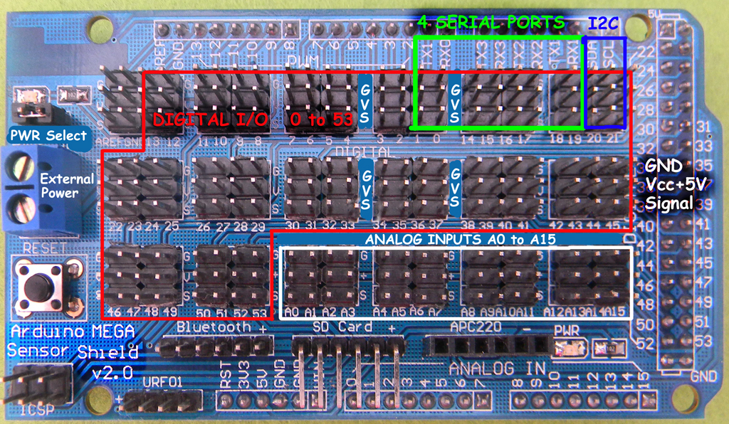
  It's difficult to manage connections and cabling to so many Inputs and Outputs. The Mega Sensor Shield HERE makes it easier.


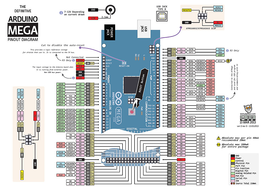
  And here's a Nice MEGA Pinout Diagram:


  zz


